In the measurements just described, the uncertainty can be broken into two broad categories:
1. Uncertainty associated with the characterization of the calibration device (such as the MN4765X)
2. Uncertainty in the measurement with the DUT
Typically the user will purchase a characterized photodiode and receive a data file describing that device’s transfer function. There is some uncertainty associated with that data based on the characterization technique.
There are different levels of characterization possible. A direct characterization using such optical techniques as electro-optic sampling (e.g., [1]) or the heterodyne method (e.g., [2]) would be termed 1st tier. It is outside the scope of this note to go into detail on these characterization techniques but they are discussed in the references and elsewhere in the literature. These 1st tier characterizations are typically performed at National Metrology Institutes (NMIs, such as NIST or NPL) or large private laboratories.
A 2nd tier standard is characterized by a laboratory based on a 1st tier standard. It would be generated using a process similar to the techniques discussed here but under carefully controlled conditions (bias, temperature, wavelength, etc.) using a 1st tier standard as the characterization device. This 2nd tier device is much more commonly available (the MN4765X is an example) and the uncertainties for a 2nd tier standard will be used in later calculations. The uncertainty penalty in going to 2nd tier device is typically small (on the order of 0.1 dB additional).
When measuring the DUT, there is an uncertainty associated just with the VNA measurement which is discussed elsewhere (e.g, [5]). Since the characterized photodiode response is then de-embedded, the characterization uncertainty must be combined with the VNA measurement uncertainty to obtain an overall value. In the case of an O/E measurement, there are actually two user measurements involved (one with a modulator and the characterized photodiode and one with that modulator and the DUT) so an additional uncertainty must also be included (note the distinction between this second level de-embed and a 2nd-tier calibration device). Typically these uncertainties are all added on a root-sum-square basis since the measurements are assumed to be dominated by uncorrelated quantities.
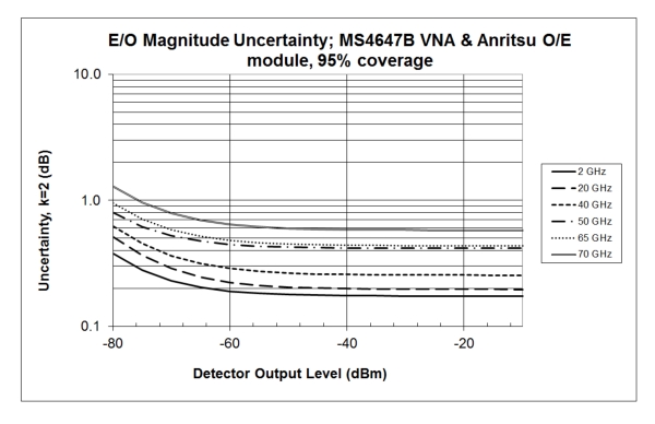
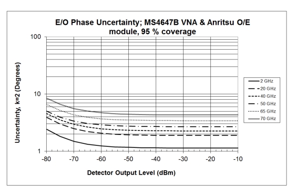
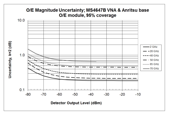
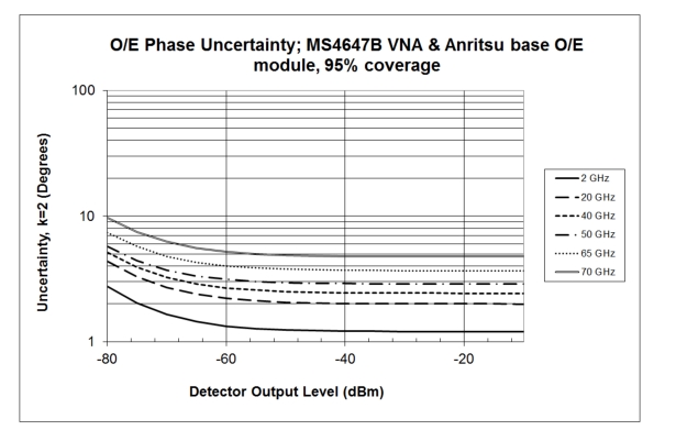
Before proceeding to some uncertainty values, it may be useful to examine dependencies. On the VNA side, S21 uncertainty is typically quite low for medium power levels but will deviate at high signal levels (receiver compression, not an issue in these measurements) and at low signal levels (effects of the receiver noise floor). Thus the overall uncertainty will be a function of detector output signal level (getting worse as the signal level gets closer to the noise floor). Results can be improved by using higher RF drive levels (keeping all devices linear) and high optical power levels (same caveat). The RF match of the modulator and photodiode will also influence uncertainties to some degree (at all signal levels) but the dependence is relatively weak as long as return loss is better than a few dB. For the plots in Figure: Example E/O Measurement Uncertainty Plots and Figure: Example O/E Measurement Uncertainty Plots, a modulator match of –24 dB at low frequencies to –15 dB at 65 GHz and a detector match of –20 dB at low frequencies to –9 dB at 65 GHz were assumed as is typical for some commercial devices. Making both matches worse by 5 dB causes an uncertainty degradation of about 0.15 dB.
On the optical side, there is little high level signal dependence as long as the devices are operating linearly. The characterized photodiodes are usually chosen to be very linear over wide power ranges to keep this from being an issue. The characterized detectors typically also have very weak wavelength dependencies; usually less than a few hundredths of a dB over 40 nm. When using a modulator as a transfer standard (as in an O/E measurement), however, it is important that the same wavelength be used in the different measurements with that modulator since much greater wavelength sensitivity usually exists in that component (although this will vary with technology). Specifications for the Anritsu MS4647X VNA and 3654D V Calibration Kit were used to calculate VNA uncertainties at various frequencies. The use of different VNAs and/or calibration kits may result in slightly different values. Characterization uncertainties of the MN4765X O/E calibration device were used for the standard part of the model. Optical system drift is included in the error model but it is assumed that all components are mechanically and thermally stable. Connector repeatability is also included in the model but all connectors are assumed to be in very good condition. The results are shown with an independent variable of photodiode output power and plotted for both magnitude and phase for the two different types of measurements. Frequency is used as a parameter. While the results for a 2-port measurement are shown here, there are normally no significant deviations in going to 4-port structures.
Generally, the MN4765X is treated as the traceable optical converter element in the uncertainty analysis since it has the most direct path to a standards laboratory. When measuring an OE device, the characteristics of the MN4765B are first transferred to a modulator (like the MN4775X converter), and then that modulator response is de-embedded from the DUT measurement. As will be seen, this additional transfer adds some small amount of uncertainty (for repeatability and additional VNA measurement reasons). A separately characterized modulator can, of course, be used as well, but, usually that will have a slightly higher starting uncertainty since an OE transfer probably occurred earlier (and one would have to include the aging of that characterization). An OO measurement will typically involve two such transfers, so the uncertainties increase a bit more.
Example uncertainty curves have been generated here that are based on using 70 GHz/1550nm version of the MN4765X as the 2nd tier calibration device. As can be seen in Figure: Example E/O Measurement Uncertainty Plots andFigure: Example O/E Measurement Uncertainty Plots, the uncertainty reaches an asymptote for detector output levels above about –60 dBm. Above this level, the dominant source of uncertainty passes from measurement signal-to-noise ratio to characterization uncertainty. The x-axes in these plots are indexed in received VNA power, so optical power, modulator optical path loss, other optical path losses, and responsivities all play a role. The ME7848A system uncertainties (see the appropriate technical data sheet) are slightly different since actual converter mismatch values and repeatabilities are used, but the trends are largely the same for all configurations within a wavelength family. There are more substantial differences between wavelengths because the first tier calibrations (by the metrology institutes) have different uncertainties per wavelength and the MN4765B behaviors vary significantly with photodiode used therein.
There is some frequency dependence for several reasons:
1. Noise floor is higher at higher frequencies.
2. The characterization uncertainty goes up with frequency.
3. The basic VNA uncertainty (due to residual mismatch, etc.) goes up with frequency.
Example E/O Measurement Uncertainty Plots
Example E/O measurement uncertainty plots are shown here for the conditions discussed in the text.
Example O/E Measurement Uncertainty Plots
Example O/E measurement uncertainty plots are shown here for the conditions discussed in the text.
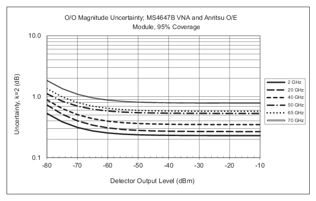
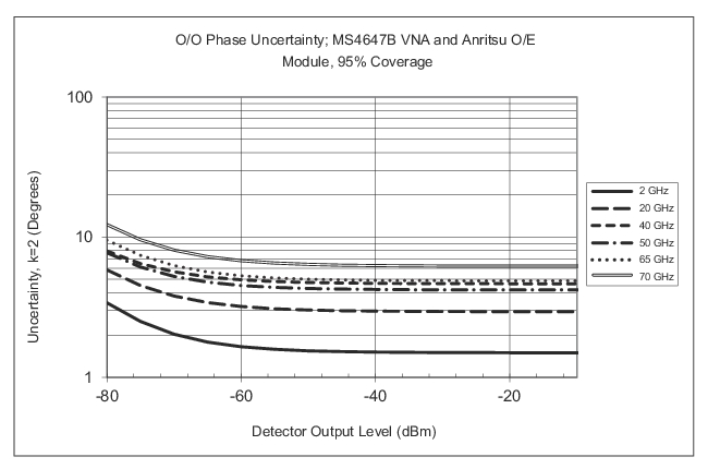
Example O/O Measurement Uncertainty Plots
Example O/O measurement uncertainty plots are shown here for the conditions discussed in the text. Optical component mismatch effects are not included.
Additional Comments on the Uncertainty Curves and Calculations
• Older MN4765As were characterized on a different VNA platform (37XXX) that had different base uncertainties particularly in terms of the noise floor at higher frequencies. The characterization data for those modules has that uncertainty built-in and hence, the optical converter measurements, even if performed on a MS464XX VNA will be somewhat elevated (by about 0.5 dB in E/O magnitude at –50 dBm and 65 GHz; less at lower frequencies and higher power levels). Uncertainties for 37xxx-based characterization and measurement are published in an older application note (e.g., [6]). The uncertainties for a MS464XX-measured but 37XXX-characterized setup will be part way between the curves published in that older application note and the curves published here.
• MN4765As were characterized to 65 GHz. There are a variety of configurations for B and later revisions including those characterized to 70 or 110 GHz for 1550 nm applications and those characterized to 70 GHz for both 1550 and 1310 nm wavelengths. Consult the technical data sheet for these models for more information on their uncertainty behaviors. In general, the trends will be similar to those discussed in the earlier example. The 110 GHz module usage is obviously of most benefit with the ME7838X broadband VNAs.
• While individual models were characterized with specific wavelengths in mind, typically the uncertainty degradation over neighborhoods of 50nm or more is very minor (less than a few tenths of a dB in magnitude). At lower RF frequencies at least, 1550-characterized devices can be used at 1310 nm with similar degradation although behaviors changes above ~ 30 GHz to 40 GHz. Consult the factory for more information.
• Different uncertainties apply for different wavelength MN4765B models (and many of those models support multiple wavelengths and the uncertainties are different for each) in large part because of differences in how those modules are characterized and in part because of differences in RF performance.
• Errors due to polarization maintenance problems or multi-moded fiber (explicit multimode fiber or single-mode fiber being used in a wavelength range that multiple modes propagate) are not included in these uncertainties. It is assumed that appropriate optical components for the application and for the intended wavelength are being used.
• O/O uncertainties do not include optical mismatch, dispersion or other forms of optical distortion. These are only representations of uncertainties related to converter characterization, de-embedding and the RF calibration process.
• All of the uncertainties are relative in the sense they are not parameterized against optical power. The characterization optical power level for the MN4765X can be provided for one to calculate absolute uncertainties but this will require a characterization of the user’s optical components. The ME7848A system does provide absolute uncertainties (see the appropriate technical data sheet), as the E/O and laser behaviors are known. An absolute responsivity uncertainty will include all of the above effects plus uncertainty in optical power and uncertainty in absolute responsivity of the paired converter (e.g., the O/E module when measuring an E/O device).