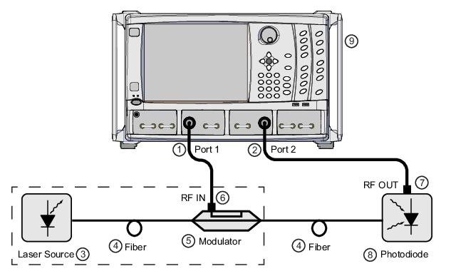
Conceptually, the job of the optical modulator is to place a microwave signal as modulation onto an optical carrier. Similarly, the job of the photodetector or receiver is to recover that modulation and regenerate the microwave signal. For a VNA-based measurement, both directions of conversion are required so that the processing can occur in the microwave or modulation signal domain. The result is a setup like that shown in Figure: General 2-port E/O or O/E Measurement Setup. The optical carrier is generated (usually) by a coherent laser source (which may be integrated with the modulator), modulation is applied, and then the modulation is recovered. Optical fiber is shown as the media in Figure: General 2-port E/O or O/E Measurement Setup but it could be some other optical guiding medium or free-space in some cases. The VNA acts as a microwave stimulus (Port 1 in the figure) and receiver (Port 2 in the figure). 3- and 4-port cases are also possible, involving multiple converters or differential ones, which will be discussed later in this chapter. Although a fiber is shown as the only element between the detector and modulator in Figure: General 2-port E/O or O/E Measurement Setup, some optical DUT may be there for O/O measurements.
General 2-port E/O or O/E Measurement Setup
In some cases, the laser and modulator may be one assembly (as is the case in the MN4775X converter). The photodiode may be integrated with amplifiers or other components into a photoreceiver.
Index
Description
Index
Description
1
VNA Port 1
6
Modulator RF IN
2
VNA Port 2
7
Photodiode RF OUT
3
Laser Source
8
Photodiode
4
Fiber
9
MS464xB VNA
5
Modulator
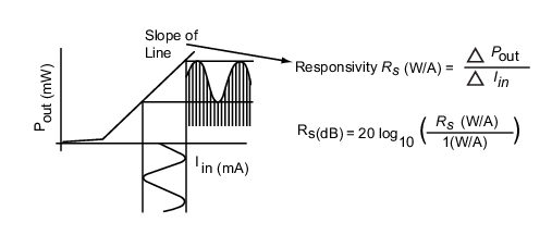
Since the measurements results will be classed as normal S-parameters, one may wonder how these relate to the actual optical behaviors of the components. In some sense, they all become relative because the conversion between domains introduces dependencies on optical laser power, optical path losses (usually small) and other absolute shifts. Thus the real measure of conversion is essentially a responsivity slope between the optical and electrical domains as illustrated in Figure: Responsivity Concept. The S-parameters that appear on the instrument display for an O/E or an E/O component then represent a relative responsivity measure (in both magnitude and phase). Often, the frequency response of this quantity is of interest as that determines bandwidth and magnitude vs. frequency plot gives this information. The phase linearity and group delay are both ways of looking at the deviation from a purely linear phase function that can be an important assessment of potential phase-related modulation distortion. Return loss of the component may also be of interest but that is a purely microwave measurement.
Responsivity Concept
The conversion parameters of the O/E and E/O devices measured with the VNA are essentially measures of responsivity.
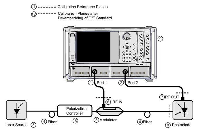
A next question may be how the measurements are conducted. The starting point is a 2-port VNA calibration as has been discussed in earlier chapters of this measurement guide. This calibration establishes reference planes at the microwave ports of the optical devices as shown in Figure: Reference Plane Placement (often coaxial ports but could be waveguide, in a fixture, etc.). The next step is the use of an O/E calibration device such as the MN4765X. That particular model is a wide bandwidth photodetector housed in a thermally controlled module with carefully designed bias circuitry. This module is characterized at a traceable facility using electro-optic sampling techniques (or references derived from that) so its frequency response (in magnitude and phase) is well-known with established uncertainties (e.g., [1] -[2]). If such a calibration device is the detector in Figure: General 2-port E/O or O/E Measurement Setup, then its effects can be de-embedded (see the embedding/de-embedding sections of Calibration and Measurement Enhancements in this guide for more general information) since those behaviors are known. This then moves the reference plane to the optical side of the photodiode/calibration detector as shown in Figure: Reference Plane Placement. Now a measurement of S21 will describe the loss and phase of the modulator alone (plus some effect of the fiber which will be discussed). This frequency response (magnitude and phase) gives the required performance information discussed earlier when combined with the microwave reflection measurement (S11 in the diagram) of the modulator RF port that comes for ‘free’ with the calibrated VNA measurement.
A polarization controller is shown in Figure: Reference Plane Placement but, technically, this is optional. Many modulator structures (including Mach-Zehnder modulators such as those used in the MN4775X converter), are polarization sensitive so at least a polarization-maintaining fiber is recommended on the modulator input.
Reference Plane Placement
A calibration is done in coax, waveguide, or some other electrical media and the de-embedding function, via the O/E-E/O measurement utility, of the VNA are used together with optical data to move a reference plane into the optical domain.
Index
Description
Index
Description
1
VNA Port 1
7
Photodiode RF OUT
2
VNA Port 2
8
Photodiode
3
Laser Source
9
MS464xB VNA
4
Fiber
10
Polarization Controller
5
Modulator
11
Calibration Reference Planes
6
Modulator RF IN
12
Calibration Planes after de-embedding of O/E Standard
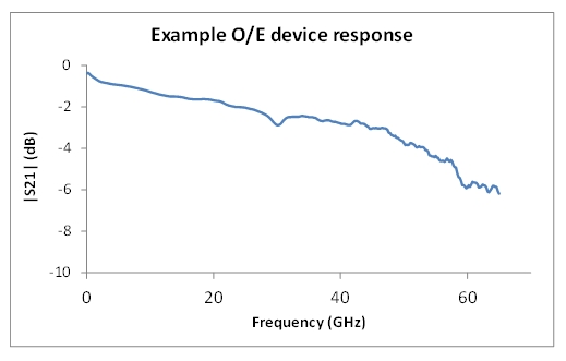
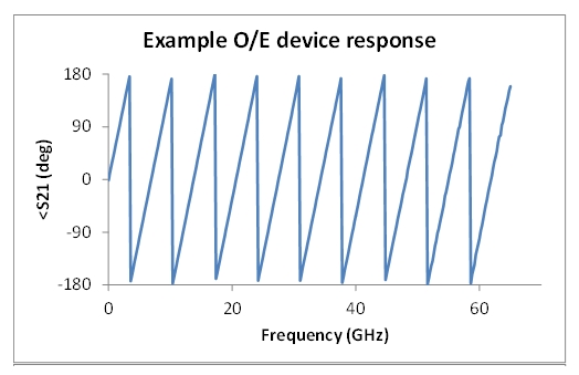
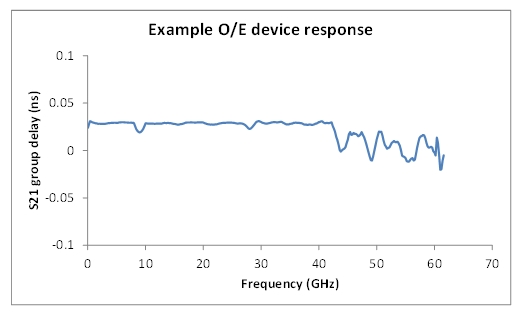
An example plot of the conversion response of a 50 GHz photodetector is shown in Figure: Characteristics of Example O/E Device. From the magnitude response, the 3-dB bandwidth is indeed around 50 GHz but the roll-off is sufficiently slow that this device is commonly used beyond 65 GHz. The phase response is also shown in the figure but the linear portion has not been removed. The group delay plot (derivative of phase with respect to frequency) is often a more convenient way of looking at the phase behavior. Towards 50 GHz, there are some deviations from flat group delay (equivalent to deviations from linear phase) that are not surprising in view of the device’s bandwidth. If being used as a characterization device, these deviations are not important since they can be well-characterized (to beyond 65 GHz in this case).
Characteristics of Example O/E Device
If one now wanted to measure a different O/E device (not a calibration module), one could then insert that detector into the setup of Figure: Reference Plane Placement and instead now de-embed the modulator response that was just found. In this case, because it is a second level de-embed, there may be some elevation of uncertainties that will be discussed. One could also obtain an E/O calibration device and use that instead in a one-step process.
The de-embedding (or sequential de-embedding) steps form the basis of this O/E-E/O measurement utility. The key points are controlling traceability and uncertainties throughout the process when multiple devices are being used, to control match so minimal additional artifacts are introduced, and to not try to de-embed what cannot be de-embedded. This last point is important in that inner-plane (optical) match is not known and the transmission path is unilateral anyway, so there are no multiple reflections within the DUT assembly to remove.
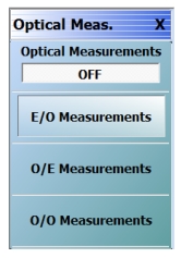
Optical Measurements Menu
All of these measurement aids are available under the Perform Optical Measurements button located on the MEASUREMENTS menu (Navigation: MAIN | Measurement | MEASUREMENT | Optical Measurements | OPTICAL MEAS. menu). As might have been guessed from the previous discussion, these approaches naturally separate based on whether the target is an O/E device (e.g., detector or receiver), an E/O device (e.g, modulator), or an O/O device (e.g, coupler, amplifier, or filter, etc). The menu selections, as shown in Figure: OPTICAL MEASUREMENTS Menu delineate that choice.
OPTICAL MEASUREMENTS Menu
On the Optical Measurements menu are the three selections based on which type of device is to be solved for.
A certain class of purely optical (O/O) measurements can also be made where both the detector and the modulator have been de-embedded. One essentially performs the steps for both the E/O and O/E measurements in series to place the reference planes in the optical domain. This is still a microwave/millimeter wave frequency response measurement so the O/O measurement is really a measure of the response to changing modulation bandwidths and, as such, is most suited to relatively narrowband optical devices such as amplifiers, filters, couplers, resonators, etc. For example, it would be unusual for a patch cord to show variation over a millimeter wave modulation bandwidth (unless it had some particularly unusual distortion properties). Also, mismatch in the optical domain is not correctable with this technique and, if the fiber runs are long, it is possible that ripple will occur on the scale of millimeter wave frequencies.
All of the measurements in this chapter work by using information about optical converters to modify an RF calibration coefficient set on the VectorStar VNA. This is exactly how conventional de-embedding works but the optical variants of this process take additional steps to handle the unilateral nature of the optical system (one cannot apply RF to the detector and usually expect RF to be produced by the modulator) and some differences in match terms. As with regular de-embedding, the optical modification to the calibration coefficients can be turned on and off. Turning the Optical Measurements to OFF will cause the original RF calibrations coefficients to be loaded. Returning Optical Measurements to ON will reload the modified coefficients. Both sets of coefficients are stored as part of the setup file.