The flexibility of the MS464xB equipped with Option 35 and Option 42 enables a very wide array of pulse generation and measurement configurations.
In the area of pulse generation, four internal pulse generators (with 3.3 V logic levels) are available for use anywhere in the test system. In addition, external pulse generators can be included in the test system and synchronized to the internal system to provide even more options. Pulses may be used to control bias, RF modulators, gain control systems, state control systems and a variety of other subsystems in the DUT or the measurement environment.
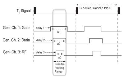
Pulse Generator Example
As an example, consider a power FET measurement where it is desired to pulse both gate and drain biases as well as the RF. Since this example is of a high power device, the sequencing of these events is important. Both for thermal reasons and for understanding bias transients, all of the biases will be pulsed. A drawing of the pulse relationships is diagrammed in Figure: Example Pulse Generator Configuration.
Three of the internal pulse generator channels are being used with the first two feeding bias switching circuitry (external to the VNA) and the third feeding an RF modulator (available in the pulse modulator test sets). All pulse generators share the same PRF but have independent widths and delays—all set with a resolution of 2.5 ns.
For this example, one may want to perform a pulse profiling measurement and Tstart might be aligned with delay 3, or just prior (so profiling begins when RF is first applied to the DUT), and Tstop may be a slightly larger value than delay 3 added to the pulse generator’s pulse width (profiling ending shortly after the RF is shut off).
Example Pulse Generator Configuration
The pulse outputs are relatively high speed and use high current drivers, so impedances down to 50 ohms are supported. It is recommended to keep series resistance under ~10 ohms for common logic families when driving a 50 ohm load.
In the example above, each pulse was discussed as a single pulse per pulse repetition interval. Doublet, triplet, quadruplet and busted pulses are all permitted independently per generator and per channel. The timing relationships are shown in Figure: Timing Relationships for Multiple-pulses-per-PRI Signals.
From the point-of-view of the measurements, timing is still relative to the T0 synch rising edge. For the doublet, triplet, and quadruplet situations, all of the widths and delays are independent (although not all are labeled in the figure for clarity). For the burst situation, all sub-pulse widths (w1) are the same and all intra-sub-pulse gaps are the same (defined by the period p and the width w1).
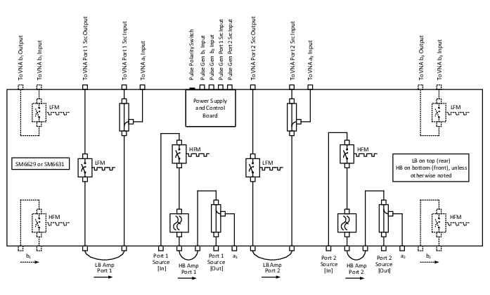
To cover a full 70 kHz to 70 GHz range with pulse modulation and to support the block diagram of the MS464xB Series, the modulation paths are split into above and below 2.5 GHz (high frequency modulator [HFM] and low frequency modulator, [LFM] respectively) with access ports on the front and rear panel for easy connection to the VNA.
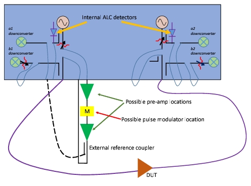
As suggested by the block diagram in Figure: Block Diagram: Four Modulator Version of the Pulse Modulator Test Set, the source side modulators include additional reference couplers that can be fed into the reference loops of the VNA to provide ratioing against a pulsed signal. This can be useful to ratio out potential ringing effects of the modulator. In many cases, these coupled paths do not have to be used and all ratioing can be performed against the usual non‑pulsed stimulus signals. Access loops are also provided to allow for amplification on the drive paths, which may be needed in higher power applications (for example several watts of DUT input power).
Block Diagram: Four Modulator Version of the Pulse Modulator Test Set
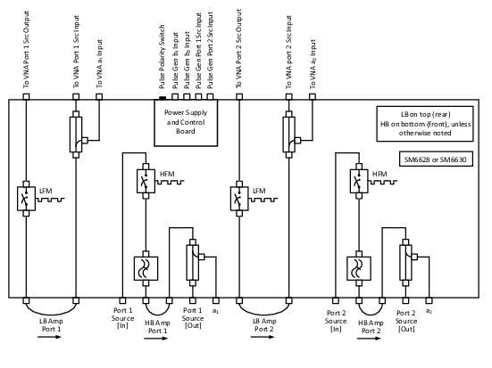
Block Diagram: Base model of the Pulse Modulator Test Set, Without Receiver-side Modulators
The most common applications will use only the source loops in order to provide stimulus modulation. In this case, only two cables per port are actually needed (two on the front for > 2.5 GHz and two more on the back for < 2.5 GHz). The source signal (post-ALC detection) is routed down to the test set and then sent back up to the VNA to pass through the test coupler. The extra reference coupler in the test set can be used to route into the reference receivers in the VNA for stimulus ratioing as discussed above.
The receiver-side paths of the pulse modulator test set are particularly useful in certain antenna applications where the transmit leakage pulse may be large enough to compress the receivers.
Note
Pulse modulator test set versions with maximum frequencies of 40 GHz and 70 GHz are available.
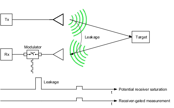
Receiver Gating Using the Receiver-side Modulators
Receiver Gating
With co-located transmit and receive antennas (Tx and Rx), sometimes there is leakage of the transmitted signal into the receiver. If the power levels are high enough, they will compress/saturate the receiver. If the leakage from the transmit pulse is earlier (in time), than the return pulse that is of analysis interest, then receiver gating can be beneficial. In some sense, this is a receiver‑gating process and is illustrated in Figure: Receiver Gating Using the Receiver-side Modulators. An RF modulator can be used to prevent this leakage pulse from being processed by the receiver so one can concentrate on the pulse from the target or some other object.
This type of special receiver‑gating is applicable to all measurement methods and is more of a tool to prevent measurement distortion rather than a tool for acquisition in itself. There may be connectorized as well as antenna-based situations where multiple pulse arrivals of different amplitudes are possible.
For any physical pulse modulator, the most interesting timing parameters are rise and fall time and latency. The former is normally set by the modulator drive circuitry and the physics of the modulator itself. For the PIN and FET modulators in the pulse modulator test set, this time is typically < 4 ns (based on 10 % to 90 % transition).
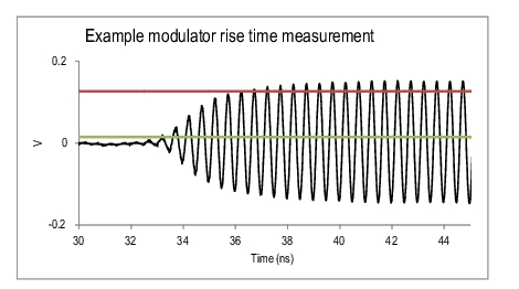
The rise/fall time limits the minimum stimulus pulse width (or receiver-gate width in the case of Figure: Receiver Gating Using the Receiver-side Modulators). Latency is the delay between the incoming video pulse edge and the RF pulse edge and is largely set by cable and logic delays. For a typical setup with the pulse modulator test set, this latency is on the order of 35 ns. Since the latency is constant, it can be accounted for in the pulse setup by adjusting pulse position timing. An example detected response using the stimulus modulator in the pulse modulator test set is shown in Figure: Example Pulse Response Plot of an Anritsu Pulse Modulator Test Set.
Example Pulse Response Plot of an Anritsu Pulse Modulator Test Set
An example pulse response plot of an Anritsu pulse modulator test set (stimulus path). The latency of about 35 ns and rise time of about 3 to 4 ns are evident. The waveform was measured with a 50 GHz bandwidth sampling scope to get adequate time resolution.
Note
When using the test set modulators, the polarities of the pulses applied are important. To allow the test set to remain connected when not being used, the modulators were configured to be in a pass-through state with logic low. Because of this, the pulse input must be inverted so that RF power is applied when the logic is low.
While pulsed power calibrations are discussed in Calibrations, a hardware setup consideration involves how the actual power leveling process occurs, particularly when pre-amplifiers are used. By default, the leveling detection node is within the VNA as part of the reference coupling system so it is always before the source loop and before any pulse modulation (and is not included with injection into the reference loop). This is adequate for many situations but if a preamplifier is being used, it may be desirable for the leveling loop to remove any drift of the pre-amplifier. Option 53 (external ALC) helps with this by allowing the use of an external detector. If the pre-amplifier is after pulse modulation, this can create a problem since the detected power will be based on average power which (a) may be a dynamic range problem for the detector if the duty cycle is low or (b) may not be optimal if one wants to level, for example, peak power, to minimize the chance of device damage. For these reasons, two additional software-based ALC detection schemes are available (per-point and per-sweep).
The central concept is that, if a reference coupler is placed correctly (see Figure: Pre-amplified, Pulsed Measurement Setup with External Reference Coupler), we have information about the signal level at every point of the pulse and can use this as the basis of leveling in a software-loop sense. Note that the pre-amplification can be before or after pulse modulation (and may change depending on power levels, pre-amplifier characteristics and modulator behavior).
Pre-amplified, Pulsed Measurement Setup with External Reference Coupler
A pre-amplified, pulsed measurement setup is shown where an external reference coupler is used to enable an enhanced leveling mode.
Other configurations are possible:
• If no reflection measurements (or full calibrations) are needed, the source loop does not need to be used and the pre-amplifier/modulator/coupler assembly could be connected to the VNA test port.
• The pre-amplifier assembly could be attached to the test port and a dual directional coupler (or two couplers) could be used with the reflected signal going to the b1 input port.
• A reverse configuration is, of course, possible.
As alluded to earlier, it would be possible to place an external ALC detector (Option 53) on this reference coupler and that would at least allow the leveling system to capture drift of the pre-amplifier(s). A potentially better option uses the internal receivers to instead help with the leveling job since the data can be analyzed at the desired time window within the pulse. This becomes a software-leveling loop of sorts but it is done in a 2-tier style: an actual diode detector (whether internal or external) is still used to control the analog loop, but now the data (from either the a1 or a2 receiver path) is used to adjust the loop settings to help maintain a desired power level at a particular point or window in the pulse.
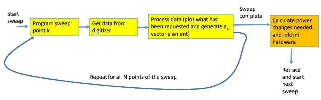
The simplest version of the leveling is termed per-sweep and is available in all pulse modes. At the end of each sweep, the a1 or a2 values (which depends on the driving port) are then compared against the target value and the ALC hardware entries changed to being the value closer to target on the next sweep. The sequence of events is shown in Figure: Sequence of Events for the Per-sweep Method of Software Pulsed Leveling. It is called per-sweep since, at least in the case of the PIP mode, the power levels are adjusted only at the end of each sweep (in profiling and P2P, each measurement cycle is a sweep). There is no appreciable overhead to measurement time with this per-sweep leveling but it will only correct for power outputs drifting on the scale of sweep time or longer.
Sequence of Events for the Per-sweep Method of Software Pulsed Leveling
The power levels are adjusted at the end of every sweep.
The target value mentioned earlier requires some explanation. If no power calibration is applied, the target will be the ALC set value (so a -15 dBm entry will try to get the a1 or a2 values to -15 dB so obviously a receiver calibration helps make these values meaningful). If a power calibration is applied, the system will record the a1 and a2 values right after calibration or leveling activation and use those as targets for all subsequent sweeps. The premise is that the power calibration will be quite accurate just after calibration and we wish to maintain those values. Note that the pulsed power calibrations discussed in Calibrations make the most sense for this setup.
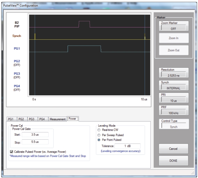
If the drift rate is much faster (or a very long sweep is needed), per-point leveling may be useful and is available for the PIP mode. In this case, a pre-measurement is done at each point in the sweep for a1 or a2 and the power is immediately adjusted in an iterative fashion to get the values closer to target (iteration limit is 20 and the tolerance (leveling convergence accuracy) can be changed by the user (default is 1 dB, tighter than a few tenths may require a lower IF bandwidth)). After convergence (or iteration limit exceeded), the full set of data is used for the pulse measurement and we move on to the next sweep point. The sequence of events is shown in Figure: Sequence of Events for Per-point Software Leveling and the leveling selection/tolerance entry field are shown in Figure: PULSEVIEW CONFIGURATION Dialog Box.
Sequence of Events for Per-point Software Leveling
The system tries to force the power level to converge to the target at each sweep point before keeping the data and moving on to the next point.
PULSEVIEW CONFIGURATION Dialog Box
Set up for per-point leveling and the power calibration set to analyze the middle of the pulse (which runs from 3-6 microseconds from synch in this example). Note that the convergence tolerance (1 dB from target here) is only shown when per-point leveling has been selected.
The target values are the same as discussed for per-sweep leveling. Because multiple measurements are done per point, the overall measurement time will increase but this may be the preferred mode if the power accuracy during the measurement is critical and the pre-amplifiers are prone to significant and/or rapid drift.
Note
When recalling a setup in per-point or per-sweep leveling with a user power calibration, this system needs to re-acquire the target values and will attempt to do so on the first sweep after recall. If an appropriate setup was not in place at that time (e.g., the signal to couple off to the reference receiver on the VNA was not connected), the user can refresh the target (force a new target acquisition) using the 'Refresh Leveling Ref.' button on the POWER >> OTHER SETUP menu after the setup is correct. One may want to do a new power calibration if the setup has changed, and that will automatically store new target values. If a power calibration is recalled on its own, a new target value acquisition is also needed.